TV160 Full HD LVDS Turn VGA LEDLCD TV Motherboard Tester Tools Converter Hot
TKDMR TV-160 Generation of LVDS Turn VGA Converter With The Display LCD/LED TV Motherboard Tester Mainboard Tool
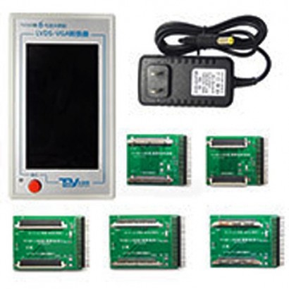
Manual of Sixth-Generation LVDS-VGA Converter (Attached with device)
Thanks for choosing Sixth-Generation LVDS-VGA Converter (Display screen version)
developed by TD Please read this manual carefully before using. During LCTV
maintenance and production, the mainboard is required to be connected to a screen for testing;
however, due to miscellaneous mainboard specifications, various screens are required for
maintenance or production. In this case, this converted is developed to reduce the pressure of
manually installed screen and prevent the screen damage caused by the output signal of mainboard
fault which leads to tremendous loss. Taking this into consideration, this converter is able to
display LVDS from the mainboard directly or convert it into VGA for output. Besides, it is able to
be connected to a displayscreen for maintenance and commissioning.
To test the motherboard than 32 LVDS signals, comes with display. After the host first powered on, and then use the original machine screen line, then the corresponding adapter plate, in the case of a short circuit board did not give the board power adapter plate lights, and then inserted into the adapter plate converter on the host, this time will be able to host the display shows the image output board.
I. Characteristics of this conversion board
1. Furnished with 4.3" display screen, it is able to display LVDS image directly from the
mainboard, supporting external VGA.
2. It supports LVDS signal with various resolution ratios (60Hz, 120Hz and 240Hz) of single or
dual shielded wire.
3. It outputs uniform VGA signal (1280*720/60HZ) which is able to be connected to various
display, supporting CRT, liquid crystal and TV display (favorable compatibility).
4. The input interface features anti-static design with better anti-static capacity.
5. Convenient conversion among various LVDS formats.
6. Wide power input design, with 5V-12V adapter.
II. Packing list and standard accessories
Note standard accessories only include two normal shielded wire conversion boards, one
for two-interface with high definition and other for four-interface with standard definition. These
two conversion boards are compatible with most shielded wires on the market. Additional FFC,
special sanxing interface and another three mainboards are optional as shown below:
III. Select a conversion board (Please log in http://www.aliexpress.com/store/1937268 to inquire and purchase)
Note these three shielded wire conversion boards are not standard accessories, but they can be
purchased. The difference is that sanxing standard-definition conversion board with two
interfaces is thicker than the interface of configured standard-definition conversion board. The
other two FFC interfaces aim at conversion board with partial screen body being customized with
FFC interface. They have the same sequences with two standard conversion boards, but the
interface is FFC. The usage is shown at the back of manual.
IV. Functions about host of converter
Description of input mode conversion
Definition of LVDS input interface
Description of input mode conversion
This converter supports complete LVDS formats and supports conversion of various
resolution ratio input (6bit, 8bit, 10bit) into VGA signal (1280*720/60HZ), with favorable
compatibility with various displays. Conversion of LVDS signal formats is realized by pressing
the mode button circularly.
Parameter table of resolution and format of converter
No. Resolution LVDS format No. Resolution LVDS format
1 800*600 VASA, JEIDA 8 1280*720 VASA, JEIDA
2 1024*600 VASA, JEIDA 9 1600*900 VASA, JEIDA
3 1280*800 VASA, JEIDA 10 1400*1050 VASA, JEIDA
4 1280*1024 VASA, JEIDA 11 1680*1050 VASA, JEIDA
5 1366*768 VASA, JEIDA 12 1600*1200 VASA, JEIDA
6 1024*768 VASA, JEIDA 13 1920*1200 VASA, JEIDA
7 1440*900 VASA, JEIDA 14 1920*1080 VASA, JEIDA
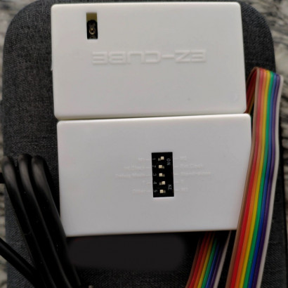
1. It is prohibited to insert a shielded wire conversion board into a converter first. Instead, it
should be connected to a TV mainboard directly before switching on the TV mainboard. This
operation easily leads to shielded wire insertion fault and component damage. Please operate it
based on the following steps
2. Do not insert a shielded wire into a converter first. Instead, please insert the original shielded
wire of a TV mainboard into the converter. During insertion, LVDS signal wire sequence should
be aligned. After switching on the TV mainboard, the small board indicator light is on, indicating
that the termination of the shielded wire (wire sequence) is correct. Then insert the converter. It is
prohibited to insert the converter inside if the small indicator light is off; otherwise, the converter
might be damaged caused by the screen power supply entering LVDS input pin.
3. Generally, the single-route LVDS signal is able to be connected 0~3 (connection of group wire
4 is not necessary) in Group A and clock input by selecting LVDS wire. It is possible to connect 5
pairs of LVDS wire input. LVDS signal of Group A is able to support the resolution ratio up to
1366*768. LVDS with two- or four-route is able to be connected to this group only.
4. The LVDS input rule of this converter follows PCB wiring rule of LCD TV produced by
Skyworth, which conforms to standard of LVDS format in the industry of color TV.
5. This converter adopts wide power supply at 5V-12V (1A) and supports portable power source at
5V/1A, so its convenient to carry for test.
6. Attention: LVDS input end of this converter should not have the screen power connected to any
pin of the LVDS input end; otherwise, it might damage the main chip of the converter. The main
chip damage incurred by this falls beyond the guarantee scope.
V. Schematic diagram of converter connection
Manual of Shielded Wire Conversion Board of Sixth-Generation LVDS-VGA Converter
During mainboard maintenance or commissioning, the original TV shielded wire might not
match this LVDS-VGA converter input interface. This issue is able to be solved by the shielded
wire conversion board. The high definition interface of the shielded conversion board adopts
original imported interface, featuring long service life. The conversion board is sold as an
accessory of the LVDS-VGA converter. Refer to the following drawing description for the
shielded wire conversion board.
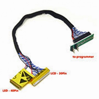
Diagram of usage of shielded wire conversion board
Step 1 Do not insert the conversion board into the converter. Instead, insert the original shielded
wire of TV mainboard into the corresponding shielded wire interface in the conversion board.
Note: the corresponding interface is based on the twisted-pair position of the shielded wire and the
position of small board LVDS paired wire, i.e. insert it correspondingly. Different shielded wire
should be inserted into different interfaces.
Step 2 Use one hand to press LVDS flat socket tightly and use the other to clench both ends of the
shielded wire to insert it in. The figure above is the high definition shielded wire interface. The
standard definition shielded wire interface follow the such insertion method. (Note: operation of
five small boards are basically identical. During connection, attention should be paid to the wire
sequence. Align the power supply before aligning the twisted-pair LVDS wire of a shielded wire and the paired signal wire of a small board.)
Step 3 Supply power to the TV mainboard. With a correct connection of a shielded wire, the indicator on
the small conversion board will be on; otherwise, it means connection of the shielded wire is
incorrect or the mainboard is not switched on. (Note: please inspect whether the mainboard screen
power supply (5 V/12 V) enters the right output pin; if it is, it will lead to a converter damage.
About an unfamiliar mainboard, a multi-meter should be used to inspect whether the contact pin
enters the screen power supply 5V/12V)
Step 4 It is able to be inserted (its front faces upwards) into the input base of LVDS ?VGA only if the
indicator on the shielded wire converter is on.
Step 5 After connection, if the mainboard of TV is normal, the display or external display on converter
will display the image of mainboard of TV.
If there is no image, check if the shielded wire is connected well or if any damage of mainboard.
In case of a blurred image, press the mode conversion button repeatedly to convert to various
modes till the image is normal.
To facilitate the mainboard testing on site, a portable power source is able to be used to supply
power to the converter. It is actually measured that Mi 10400 power (portable power from other
brand is able to be selected) is able to supply power to this converter for 15 hours, fully
conforming to testing requirements
Precautions of using converter
1. Please follow aforementioned operations strictly.
2. Firstly connect a mainboard with the shielded wire conversion board, with attention paid to the
wire sequence. Then switch on the TV mainboard, if the indicator on the shielded conversion
board is on, it means connection between the mainboard and the shielded wire board is correct;
otherwise, it should be re-inspected
3. With correct connection between the shielded wire conversion board and the mainboard, insert
the shielded wire conversion board (front faces upwards) into the LVDS converter (refer to the
figure above) before putting the TV mainboard and the converter to switching on status.
4. In case of a blurred image, press the mode conversion button repeatedly to convert to various
modes till the image is normal.
5. This converter supports various LVDS formats (60Hz, 120Hz and 240Hz). About a mainboard
with two shielded wire, one wire alone is required to be connected to the high definition
conversion board instead of both wires. Besides, it is able to convert required image.
6. Please follow aforementioned operations strictly!
Accessories
Standard accessories include two conversion boards, one for two-interface with high definition
and other for four-interface with standard definition. These two conversion boards are compatible
with interface of 32and 58 display screen.
TV160 Full HD LVDS Turn VGA (LED/LCD) TV Motherboard Tester Tools Converter Hot